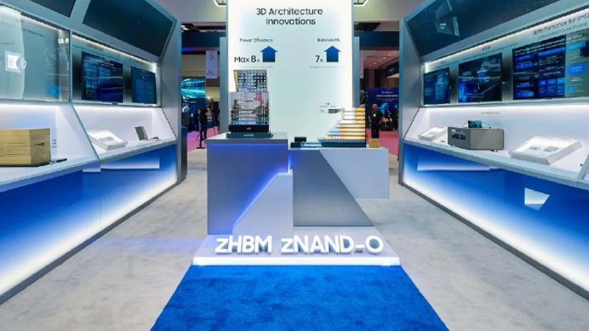

AI systems are demanding ever more speed and bandwidth from memory, both inside data centers and on the devices themselves. Samsung, one of the world's leading memory manufacturers, is responding by developing its Z-NAND technology in three separate variants: Z-NAND-O, Z-NAND-T and Z-NAND-I.
The Z-NAND-O concept made its first public appearance at an event held in August. Each of the three versions puts a different performance metric at its core.
Z-NAND-O: built for on-device AI
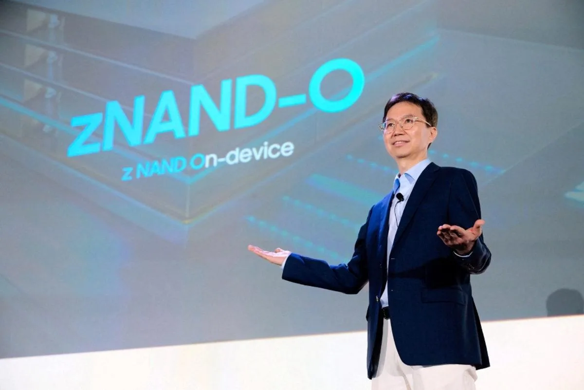
Z-NAND-O is being designed for AI workloads that phones and other mobile devices run on their own hardware. NAND flash is the non-volatile memory that stores data in smartphones, SSDs and data center drives, so faster variants have a direct impact on how quickly AI features respond. The Z-NAND-O structure places NAND chips vertically on top of one another in stacks of four or eight layers, aiming to speed up instantaneous data transfer while pulling power consumption down.
Z-NAND-T and Z-NAND-I for the data center
Z-NAND-T stands out with high processing throughput and wide data flow. Its target audience is AI data centers, which need to move enormous volumes of data in a very short time.
Z-NAND-I, by contrast, is aimed at raising the number of input/output operations completed per second. The goal is a performance uplift in database and AI server environments where large numbers of read and write requests are handled at the same time.
SK Hynix is moving in the same direction
Samsung is not alone in this race. Rival manufacturer SK Hynix is preparing a series of its own under the name “AI-NAND Family”. Within that family, AIN P centers on performance, AIN D on storage density, and AIN B on bandwidth.
The memory giants' AI-focused split signals that different workloads now call for memory solutions tailored specifically to them.






Comments (0)
No comments yet. Be the first!