
Samsung used its Global Memory Innovation Forum in China to lay out an ambitious storage roadmap, headlined by two new enterprise SSDs — including what the company calls the world's smallest 256 TB SSD — and a next-generation V-NAND architecture with more than 400 stacked layers.
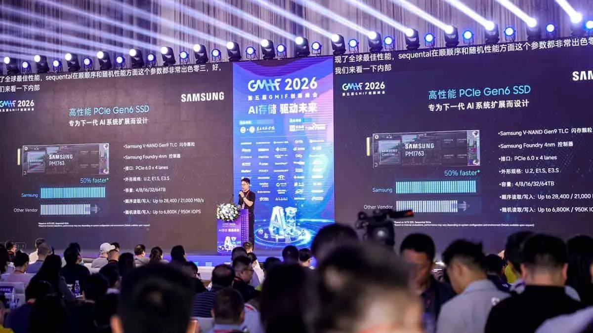
Kevin Yoon, Executive Vice President and CTO of Samsung Memory China, delivered the keynote. In his view, the shift toward autonomous systems and multi-agent AI demands a fundamental rethink of memory architectures. Samsung's answer, he argued, is a pair of enterprise SSDs designed to take the load off GPU memory.
Two new enterprise flagships
The performance-focused model is the PM1763, which supports the PCIe Gen6 interface. Sampling is planned for the fourth quarter of this year.
The second drive, the BM1773, pushes capacity to the limit. Built on an ultra-dense QLC structure, it reaches 256 TB of storage — a global record in its size class.
A 60% leap on the silicon side
Raw silicon was another highlight of the forum. The V10 BV-NAND architecture, based on a vertical bonding technique, reaches more than 400 stacked layers. Samsung says it boosts bit density by roughly 60% compared with the current generation, a significant step forward in storage efficiency.
Also on show was the zNAND-O architecture, developed for client devices. It packages processing units directly via a UCIe interface and promises 10 times higher bit density than standard DRAM, along with better read efficiency.
Samsung's efforts did not go unnoticed: as part of GMIF2026, the company received the "Outstanding AI Memory and Storage Industry Leadership Award."


Comments (0)
No comments yet. Be the first!